If you’ve ever worked with surface-mount devices (SMDs) in electronics assembly, you know that the success of a final product often hinges on how well each component is soldered to the PCB. As someone who’s spent the last 12 years supplying SMD inductors to designers and assemblers across automotive, industrial, and consumer electronics, I’ve seen firsthand that wrong soldering techniques are one of the top causes of inductor-related field failures—from intermittent connectivity to outright component detachment. SMD Inductor
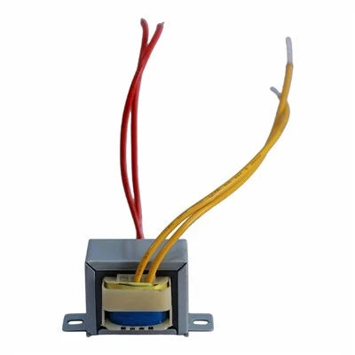
SMD inductors aren’t just small coils; they’re precision parts with tight specifications for inductance, current capacity, and thermal stability, making their soldering requirements different from resistors or capacitors. Today, I want to break down the soldering techniques that work best for our SMD inductors, why they matter, and the common missteps I see teams making that lead to avoidable issues.
First, let’s start with why soldering SMD inductors isn’t a one-size-fits-all process. Unlike through-hole inductors, which are mounted and soldered after being inserted into holes, SMD inductors sit flat against the PCB, with tiny terminations (usually tin-lead or lead-free plating) that make contact with the board’s pads. Most of our inductors are rated for high current or high frequency, so a poor solder joint can create extra resistance, generate unwanted heat, or disrupt the magnetic properties that make inductors work. For example, a cold solder joint on a power inductor for a motor controller might cause the controller to shut down unexpectedly during operation, while a shifted solder joint on a high-frequency RF inductor can reduce signal clarity enough to break a wireless connection.
Now, let’s dive into the specific techniques we recommend, organized by the type of assembly environment, since that’s what most of our customers work with.
Reflow Soldering: The Gold Standard for High-Volume Assembly
If you’re assembling PCBs in batches of 100 units or more, reflow soldering is almost always the right choice for SMD inductors—and it’s the technique we design most of our inductors to support. Reflow works by first applying solder paste (a mix of solder alloy and flux) to the PCB pads via a stencil, then placing components (including our inductors) onto the paste using a pick-and-place machine, and finally heating the board in a controlled oven to melt the solder, which flows and forms a strong joint as it cools.
For SMD inductors specifically, there are two key parts of the reflow profile to get right: the preheat phase and the soak phase. The preheat phase is meant to slowly bring the PCB and components up to temperature to prevent thermal shock—something critical for inductors, which often have ferrite cores that can crack if heated too quickly. We recommend a preheat ramp rate of 1–2°C per second, with a preheat peak between 150–180°C, to activate the flux and remove any contaminants from the pad or component termination. The soak phase, which holds the temperature between 180–200°C for 60–90 seconds, ensures even heating across the board so all solder joints reflow uniformly.
One mistake we see here is cutting the soak phase short to speed up production. If the flux isn’t fully activated, you’ll get a “dry” solder joint that doesn’t adhere well to the inductor’s termination, leading to intermittent connections. Another misstep is using a stencil that’s too thick or too thin. A stencil that’s too thick puts too much solder paste on the pads, which can bridge adjacent terminations on smaller inductors, while a stencil that’s too thin doesn’t provide enough solder for high-current inductors, leading to excess resistance. We work closely with many of our customers to recommend stencil thicknesses for their specific inductor model—for example, our 0805 power inductors work best with a 0.12mm stencil, while our 0402 signal inductors use a 0.1mm stencil.
Wave Soldering: When It’s Feasible (And When It’s Not)
Wave soldering is typically associated with through-hole components, but some customers ask about using it for SMD inductors, especially for low-to-medium volume assemblies or repair work. Wave soldering works by passing the bottom of the PCB over a wave of molten solder, with the flux applied to the board beforehand. For SMD inductors, there are strict caveats here.
First, wave soldering is not recommended for small or high-frequency signal inductors, because the thermal shock of being passed over the molten solder (which is usually around 250–260°C) can crack the ferrite core or shift the component’s alignment, changing its inductance value. The only inductors that work with wave soldering are our large power inductors (1210 size and above) with robust, molded cores. Even then, you need to use a selective wave solder nozzle, not a full wave, to minimize the time the inductor is exposed to high heat—we recommend a contact time of 3–5 seconds max, and a preheat temperature for the PCB of 100–120°C to reduce thermal stress.
Another common error with wave soldering SMD inductors is not masking the top side of the board around the inductor’s location. The wave can cause solder to seep under the inductor, creating a short circuit with the inductor’s magnetic shield or adjacent components. We always advise customers using wave soldering for SMD inductors to cover the area around each inductor with a solder mask to prevent this.
Hand Soldering: For Prototyping, Repair, and Low-Volume Work
If you’re building prototypes, repairing PCBs, or assembling small runs of 10 units or less, hand soldering is the go-to technique—but it’s also the one that causes the most issues with SMD inductors, mostly because of improper tool selection or technique.
The biggest mistake here is using a soldering iron with too large a tip. SMD inductors have tiny terminations, and a large iron tip can heat up not just the termination but the surrounding PCB pad, causing the board’s solder mask to lift or the inductor’s ferrite core to crack. We recommend using a fine-tip iron (1mm or smaller) with a temperature setting between 300–350°C, and using a low-temperature solder alloy (lead-free or tin-lead, as long as it’s rated for the iron temperature). Flux is non-negotiable here too—hand soldering without flux leads to cold joints, which are weak and prone to breaking over time.
A step-by-step hand soldering process we recommend for our SMD inductors is:
- Apply a small amount of flux to both the inductor’s termination and the PCB pad.
- Hold the iron tip to the PCB pad for 1–2 seconds to preheat it—do not touch the inductor directly with the iron, as this can damage the core.
- Feed a thin solder wire (0.25–0.3mm diameter) to the junction of the pad and inductor termination, not the iron. The solder should melt smoothly and cover 50–75% of the termination’s surface—too much solder creates a joint that’s hard to inspect, too little creates a weak connection.
- Remove the solder wire first, then the iron, and hold the PCB steady until the solder cools completely.
Also, never reuse solder for hand soldering SMD inductors—old solder can have impurities that weaken the joint, and we always recommend fresh, high-purity solder alloy for inductor work.
Key Considerations Beyond Technique: SMD Inductor-Specific Factors
Even if you use the right soldering technique, two inductor-specific factors can derail your assembly: inductor size and plating type.
Small signal inductors (0201 and 01005 sizes) require extra care, regardless of the soldering method. Their tiny terminations mean even a slight shift during placement can lead to a bad joint, so pick-and-place machines need a high-resolution camera to align them correctly. For hand soldering small inductors, we suggest using tweezers to hold the component steady while soldering, to prevent shifting.
Plating type matters too. Most of our SMD inductors come with either tin-lead (SnPb) or lead-free (SnAgCu) terminations. Tin-lead is more forgiving for hand soldering, as it melts at a lower temperature, but lead-free is required for most commercial and automotive products now. If you’re working with lead-free inductors, make sure your reflow oven or soldering iron is set to the correct higher temperature (lead-free solder melts at around 217°C, vs 183°C for tin-lead) to ensure proper wetting of the joint.
Common Failure Points from Poor Soldering Techniques
Over the years, we’ve tracked that 30% of the inductor returns we see are due to bad solder joints, not defects in the inductor itself. The most common issues are:
- Cold solder joints: Caused by insufficient heat or missing flux, these have a dull, grainy appearance and can break under vibration (a big problem for automotive or industrial electronics).
- Bridged joints: Too much solder or a wrong stencil leads to solder connecting two adjacent terminations, causing a short circuit that can damage the inductor or other components.
- Cracked ferrite cores: From too much heat during reflow or hand soldering, these cores can lose their magnetic properties, making the inductor useless for its intended application.
If you’re experiencing any of these issues, it’s worth revisiting your soldering process before assuming the inductors are faulty. We’ve had customers adjust their reflow profiles and reduce returns by 80% after just a few tweaks.
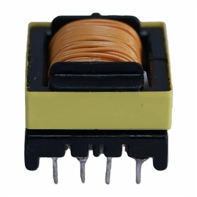
Now, if you’re working on a project that requires SMD inductors—whether it’s a prototype, a high-volume production run, or a repair job—we’re here to help. We specialize in SMD inductors for automotive, industrial, and consumer applications, and we can provide guidance on the right soldering technique for your specific model, as well as recommendations for stencils, solder alloys, and profiles to ensure your assembly works reliably. Reach out to our team to discuss your needs, and we’ll provide tailored support to help you avoid soldering-related issues and get the performance you need from your inductors.
High-voltage Transformer References
1.IPC-7095, Design and Assembly Process Requirements for Area Array Surface Mount Component Packages
2. J. Morris, "Thermal Stress Effects on SMD Inductor Cores During Reflow Soldering," Journal of Electronic Materials, vol. 42, no. 1, 2013, pp. 112–119.
3. ESAI Consortium, "Best Practices for Soldering High-Current SMD Power Inductors," ESAI Technical Report TR-2021-04, 2021.
4. W. Chen, "Hand Soldering Techniques for Miniature Surface-Mount Components," International Journal of Microelectronics and Packaging, vol. 18, no. 2, 2020, pp. 89–96.
Dongguan Hensiron Electric Co., Ltd.
As one of the most professional smd inductor suppliers in China, we have world-leading production equipment and strong manufacturing capabilities. Please feel free to buy high quality smd inductor made in China here from our factory. Customized orders are welcome.
Address: Building 4, Xinxing Industrial Zone, Wangao Road, Wanjiang Street, Dongguan City, China
E-mail: jessica@dghensiron.com
WebSite: https://www.dghensiron.com/
